RSS

New products

Display per page

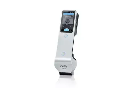
便携式接触角测量仪

表面质量控制从未如此简单可靠 便携式接触角测量仪Ayríís摆脱了因人为干预造成测量结果不同的问题,采用了开创性的技术对润湿性进行可靠的QC检测。只需单击一次,几秒钟内即可测量水的3D接触角,根据预设的质量标准,仪器会在自动验证后显示验证通过/失败的信息。Ayríís采用了先进的3D水滴投影技术可实现自动自检,且保证每个测量结果的一致性和合理性。Ayríís是一款便携的、独立的仪器,配有易于更换的充电电池和预填充液体盒,以供生产线全天候工作。
Call for pricing

TLM-SCAN+

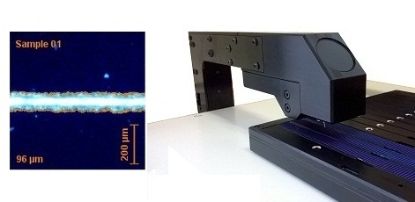
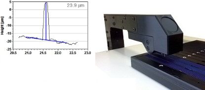
TLM-SCAN+ Contact resistivity and more This compact instrument measures contact resistivity, finger line resistance, finger width, and finger height of a finished solar cell or on test structures. Motorized in all axes it is capable of creating maps of all these methods by pushing a single button. Four point probe heads for measuring the sheet resistance of thin diffused layers and resistivity of wafers make the TLM-SCAN+ a low-cost yet fast and high-quality four-point-probe mapper.
Call for pricing

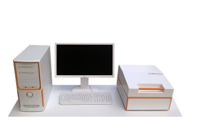
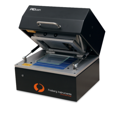
PIDcon bifacial 台式潜在诱导退化测试仪

特性 根据IEC 62804-TS标准方法 易于使用的台式设备 能够测量c-Si太阳能电池和微型模块 无需气候室 不需要电池层压 测量速度:小时到天 可测量参数:分流电阻、功率损耗、电导率、泄漏电流、湿度和温度 太阳能电池可以通过EL等进行研究 基于IP的系统允许在世界任何地方进行远程操作和技术支持
0.000 (CNY)

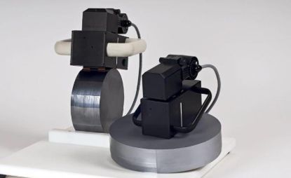
BCT-400 少子寿命测试仪

Sinton BCT-400 少子寿命测量仪 是基于涡流传感器和红外光致光电导方法直接测量单晶或者多晶硅棒体少子寿命的设备,具有瞬态和准稳态两种测量模式。该设备可探测3mm 深度范围少子寿命,并能输出不同载流子注入水平下的少子寿命值,可实现低电阻率硅单晶少子寿命测量,并能通过软件端光强偏置实现单晶缺陷密度计算。
Call for pricing

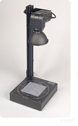
Model WCT-120/WCT-120MX -i Standard Offline Wafer Lifetime Tool

The wafer measurement instrument offering the best available calibrated analysis of carrier recombination lifetime. Fully compliant with SEMI Standard PV-13. The WCT-120 is an affordable, tabletop silicon lifetime and wafer metrology system, suitable for both device research and industrial process control. The WCT-120MX is optimized for 230mm wafer measurements. The WCT-120 instruments utilize both the QSSPC and transient photoconductance decay techniques to measure the lifetimes of wafers in the range of 10ns to greater than 10ms. The QSSPC technique is ideal for monitoring multicrystalline wafers, dopant diffusions, and low lifetime samples. The transient photoconductance decay technique is ideal for monitoring high lifetime samples at various processing steps. The WCT-120 lifetime measurement also yields the implied open-circuit voltage (versus illumination) curve, which is comparable to an l-V curve at each stage of a solar cell process.
Call for pricing

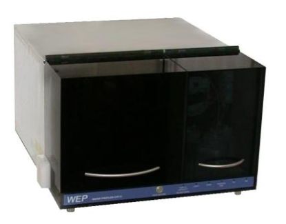
WAFER PROFILER CVP21

The Wafer Profiler CVP21 is a handy tool to measure doping profiles in semiconductor layers by Electrochemical Capacitance Voltage Profiling (ECV-Profiling, CV-Profiling) in semiconductor research or production. This ECV Profiler (CV-Profiler, C-V-Profiler) furthermore is a very good choice to analyze or develop strategies for Photo-Electrochemical Wet Etching (PEC-Etching) of semiconductors
Call for pricing
沪ICP备13027087号-6